- 您现在的位置:买卖IC网 > Sheet目录320 > DK-DEV-2AGX260N (Altera)KIT DEV FPGA 2AGX260 W/6.375G TX
�� �
�
�Chapter� 6:� Board� Test� System�
�Using� the� Board� Test� System�
�■�
�■�
�6–5�
�MAX� II� ver� —Indicates� the� version� of� MAX� II� code� currently� running� on� the� board.�
�The� MAX� II� code� resides� in� the� <install�
�dir>� \kits\arriaIIGX_2agx260_fpga\examples� directory.� Newer� revisions� of� this�
��page� of� the� Altera� website.�
�MAC� —Indicates� the� MAC� address� of� the� board.�
�MAX� II� Registers�
�The� MAX� II� registers� control� allow� you� to� view� and� change� the� current� MAX� II�
�register� values� as� described� in� Table� 6–1� .� Changes� to� the� register� values� with� the� GUI�
�take� effect� immediately.� For� example,� selecting� a� new� frequency� in� the� OCR1� list�
�immediately� changes� the� clock� frequency� on� the� board.�
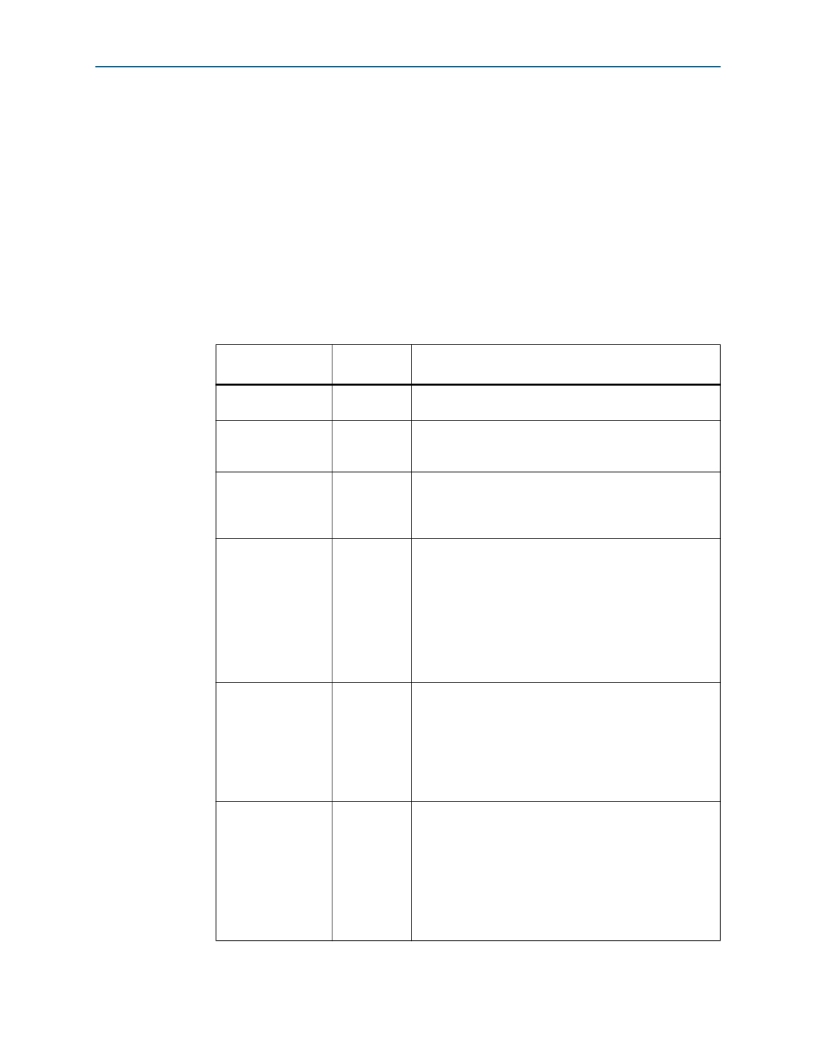
�Table� 6–1.� MAX� II� Registers�
�Register� Name�
�System� Reset�
�(SRST)�
�Page� Select� Register�
�(PSR)�
�Page� Select� Override�
�(PSO)�
�Read/Write�
�Capability�
�Write� only�
�Read� /� Write�
�Read� /� Write�
�Description�
�Set� to� 0� to� initiate� an� FPGA� reconfiguration.�
�Determines� which� of� the� up� to� eight� (0-7)� pages� of� flash�
�memory� to� use� for� FPGA� reconfiguration.� The� flash� memory�
�ships� with� pages� 0� and� 1� preconfigured.�
�When� set� to� 0,� the� value� in� PSR� determines� the� page� of�
�flash� memory� to� use� for� FPGA� reconfiguration.� When� set� to�
�1,� the� value� in� PSS� determines� the� page� of� flash� memory� to�
�use� for� FPGA� reconfiguration.�
�Holds� the� current� value� of� the� iluminated� CONFIG� LED� (D11-�
�D13)� based� on� the� following� encoding:�
�0� =� CONFIG� LED� (D13)and� corresponds� to� the� flash�
�■�
�Page� Select� Switch�
�(PSS)�
�Read� only�
�■�
�memory� page� for� the� factory� hardware� design�
�1� =� CONFIG� LED� (D12)and� corresponds� to� the� flash�
�memory� page� for� the� user� hardware� 1� design�
�■�
�2� =� CONFIG� LED� (D11)and� corresponds� to� the� flash�
�memory� page� for� the� user� hardware� 2� design�
�Determines� the� U26� oscillator� output� frequency� based� on�
�the� following� options:�
�Oscillator� Control�
�Register� 1� (OCR1)�
�Read� /� Write�
�■�
�■�
�■�
�■�
�0� =� 100� MHz�
�1� =� 125� MHz�
�2� =� 150� MHz�
�3� =� 156.25� MHz�
�Determines� the� U30� oscillator� output� frequency� based� on�
�the� following� options:�
�■�
�0� =� 100� MHz�
�Oscillator� Control�
�Register� 2� (OCR2)�
�Read� /� Write�
�■�
�■�
�■�
�1� =� 125� MHz�
�2� =� 150� MHz�
�3� =� 156.25� MHz�
�You� cannot� change� OCR2� from� the� GUI.�
�July� 2010� Altera� Corporation�
�Arria� II� GX� FPGA� Development� Kit,� 6G� Edition� User� Guide�
�发布紧急采购,3分钟左右您将得到回复。
相关PDF资料
DK-DEV-4SE530N
KIT DEV STRATIX IV FPGA 4SE530
DK-DEV-4SGX530N
KIT DEVELOPMENT STRATIX IV
DK-DEV-5AGXB3N/ES
ARRIA V DEVELOPMENT KIT
DK-DEV-5M570ZN
KIT DEV MAX V 5M570Z
DK-DEV-5SGXEA7N
KIT DEV STRATIX V FPGA 5SGXEA7
DK-DSP-2S180N
DSP PRO KIT W/SII EP2S180N
DK-DSP-3C120N
KIT DEV DSP CYCLONE III EDITION
DK-K7-CONN-CES-G
KINTEX-7 FPGA CONNECTIVITY KIT
相关代理商/技术参数
DK-DEV-3C120N
功能描述:可编程逻辑 IC 开发工具 FPGA Development Kit For EP3C120F780
RoHS:否 制造商:Altera Corporation 产品:Development Kits 类型:FPGA 工具用于评估:5CEFA7F3 接口类型: 工作电源电压:
DK-DEV-3CLS200N
功能描述:可编程逻辑 IC 开发工具 FPGA Development Kit For EP3CLS200F780
RoHS:否 制造商:Altera Corporation 产品:Development Kits 类型:FPGA 工具用于评估:5CEFA7F3 接口类型: 工作电源电压:
DK-DEV-3SL150N
功能描述:可编程逻辑 IC 开发工具 FPGA Development Kit For EP3SL150F152
RoHS:否 制造商:Altera Corporation 产品:Development Kits 类型:FPGA 工具用于评估:5CEFA7F3 接口类型: 工作电源电压:
DK-DEV-3SL150N/ES
制造商:Altera Corporation 功能描述:KIT DEVELOPMENT STRATIX II ES
DK-DEV-4CGX150N
功能描述:可编程逻辑 IC 开发工具 FPGA Development Kit For EP4CGX150
RoHS:否 制造商:Altera Corporation 产品:Development Kits 类型:FPGA 工具用于评估:5CEFA7F3 接口类型: 工作电源电压:
DK-DEV-4CGX150N
制造商:Altera Corporation 功能描述:KIT STARTER CYCLONE IV GX ((NS
DK-DEV-4S100G5N
功能描述:可编程逻辑 IC 开发工具 FPGA Development Kit For EP4S100G5F
RoHS:否 制造商:Altera Corporation 产品:Development Kits 类型:FPGA 工具用于评估:5CEFA7F3 接口类型: 工作电源电压:
DK-DEV-4SE530N
功能描述:可编程逻辑 IC 开发工具 FPGA Development Kit For EP4SE530H35
RoHS:否 制造商:Altera Corporation 产品:Development Kits 类型:FPGA 工具用于评估:5CEFA7F3 接口类型: 工作电源电压: